PVA TePla and Fraunhofer IISB Establish Joint Lab for Aluminum Nitride Substrates
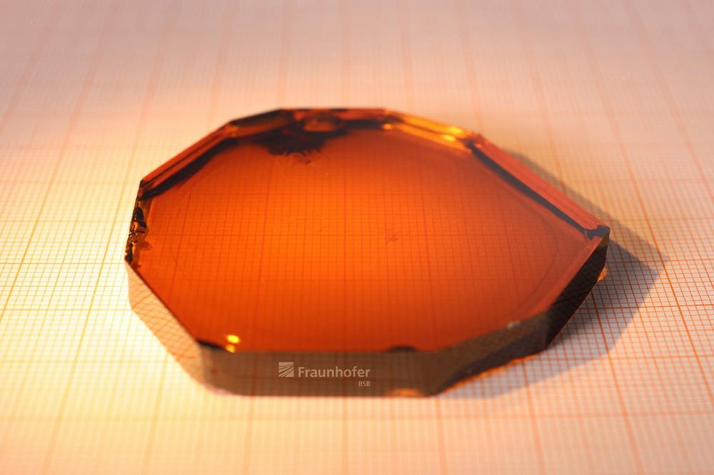
Aluminum nitride is one of the most promising materials for the next generation of high-performance electronics. As an ultra-wide bandgap (UWBG) semiconductor, AlN opens up new possibilities in photonics, power electronics, high-frequency electronics, and electronics operating under extreme conditions. To date, the shortage of high-quality, large-area, and cost-effective AlN substrates has been holding back the development of AlN-based electronic systems.
»With the Joint Lab, we are laying the groundwork to ensure a reliable supply of AlN substrates from Europe, thereby opening up new prospects for the next generation of high-performance AlN devices«, says Dr. Sven Besendörfer, group leader for nitride materials and responsible for AlN material development at Fraunhofer IISB. »Together with PVA TePla, we are contributing our expertise in industrial crystal growth, thereby creating the prerequisites for the transfer to concrete applications.«
Proven equipment technology meets proprietary process know-how
In the Joint Lab, Fraunhofer IISB is using its proprietary PVT (Physical Vapor Transport) process technology to produce 2-inch AlN bulk crystals. In this process, AlN powder is vaporized in a crucible at temperatures well above 2000 °C and deposited onto a seed crystal. PVA TePla provides PVT systems for this purpose, which are already in use worldwide for 8-inch-diameter silicon carbide (SiC) crystals and have now been specially adapted for the growth of 2-inch AlN crystals. Thanks to the process expertise contributed by Fraunhofer IISB, the PVA TePla team was quickly able to produce AlN crystals of comparable quality in its own facilities. The Joint Lab focuses on the stable small-batch production of 2-inch AlN crystals. Production is now being ramped up gradually to systematically optimize process stability, reproducibility, yield, and cost structures.
»With aluminum nitride, we are actively shaping the next generation of technology following SiC,« explains Dr. Jan Pfeiffer, Vice President of R&D at PVA TePla. »Through the Joint Lab, we can directly combine our equipment expertise with the process know-how of Fraunhofer IISB, enabling us to offer market-oriented solutions to our global customers at an early stage. Our shared goal is to stimulate market development in the AlN sector through suitable substrates and to support companies looking to enter this field as technology partners with the right equipment and corresponding process expertise.«
Strengthening European technological sovereignty through industrial scaling
The AlN crystals produced in the Joint Lab are further processed at Fraunhofer IISB into epi-ready AlN substrates and, through LZE GmbH, specifically transferred into industrial development and scaling processes. »For Europe’s semiconductor sovereignty, it is crucial that new key materials are not only developed but also rapidly transferred into industrial applications and scalable value creation. With its marketplace for cutting-edge technologies, LZE GmbH provides companies and research institutions with globally unique and open access to AlN substrates. In this way, we help ensure that promising applications for high-volume industrial markets are brought to market more quickly,« says Dr. Christian Forster, Managing Director of LZE GmbH.
At the same time, Fraunhofer IISB is driving forward the development of 4-inch, and, in the future, 6-inch AlN technology. The Joint Lab is thus laying the foundation for medium- to long-term scaling of substrate sizes. The partnership also pursues the strategic goal of pooling expertise in ultra-wide bandgap technology in Europe, reducing dependencies on key materials, and sustainably strengthening Europe’s technological sovereignty in the semiconductor sector.
The Fraunhofer Institute for Integrated Systems and Device Technology IISB is one of Europe’s leading research institutions for wide-bandgap semiconductors and power electronics systems. It serves the entire value chain of power electronics. The spectrum ranges from crystals and substrates to semiconductor devices and process tech-nologies, power electronics modules and components, and complete electronic and energy systems. Key applica-tion areas include electromobility, aerospace, sustainable energy supply, and civil security. With its solutions, the institute consistently sets new benchmarks in energy efficiency and performance, even under extreme operating conditions. The integration of intelligent, data-driven functionalities continuously opens up new application sce-narios. In this way, the IISB supports customers and partners worldwide in transforming research results into competitive products. Approximately 350 employees work at the IISB’s locations: the headquarters in Erlangen, the E|Road Center at the Cleantech Innovation Park in Hallstadt, the BioCity Campus in Leipzig, and the Fraunho-fer Technology Center for High-Performance Materials (THM) in Freiberg.
Fraunhofer-Institut für Integrierte Systeme und Bauelementetechnologie IISB
Schottkystraße 10
91058 Erlangen
Telefon: +49 (9131) 761-0
Telefax: +49 (9131) 761-390
http://www.iisb.fraunhofer.de
