sCMOS Camera Designs Push the Limits on Resolution
Pushing the limits
For a long time, the diffraction limit defined by Ernst Abbe described a natural barrier limiting the ability of optics to resolve small objects. In its original sense, the Abbe limit states that shorter wavelengths allow higher image resolution and therefore a heightened ability to observe small structural features in the image.
Although Abbe demonstrated this fundamental law in the visible range, it applies to all wavelengths of the electromagnetic spectrum, including the high-energy photons of the EUV and soft x-ray regimes. It even applies to electron-based microscopy methods. Although rules around resolution and the diffraction limit are still valid when resolving images with EUV, soft x-ray, and high-energy electrons, it is possible to push the resolution further, enabling images of fine structural features, as well as the dynamics in biological processes or materials.
Although electron microscopy uses a significantly shorter wavelength compared to EUV and soft x-ray (and therefore offers comparably higher resolution), most biological samples and materials are directly affected by this (invasive) type of irradiation, making it incompatible for nondestructive testing methods used in medicine, biology, and polymer science. In contrast, EUV and soft x-ray contain less energy, and thus they allow the repeated exposures required to enable live-cell imaging or simplified sample preparation.
In addition to scientific applications, EUV and soft x-ray have also found uses in industry. For instance, these forms of radiation have significantly benefited semiconductor chip production by continuing to fulfill Moore’s law on the progression of transistor density. Due to its short wavelengths, EUV enables chipmakers to etch ever smaller transistors and other electronic components on integrated chips. This helps reduce the complexity of chip fabrication while accelerating it, allowing chipmakers to produce more efficient integrated circuits at a reduced cost. Moreover, new imaging concepts such as EUV ptychography enable inspection of semiconductor material quality with significantly higher speed and accuracy.
Occupying the lower end of the electromagnetic spectrum, x-rays bridge the gap between the EUV spectrum and gamma rays. The lower-energy soft x-ray region covers the spectral range from 0.2 to 12 nm, while EUV spans the spectrum from 10 to 124 nm, with a central wavelength of 13.5 nm. Naturally, all stars produce EUV light, including our own. Luckily, most of this high-energy, carcinogenic radiation is filtered out by small molecules in our atmosphere — such as carbon, nitrogen, and water — allowing life to persist on Earth. Importantly, it is these molecules’ high absorptivity of EUV and x-ray energy that makes them attractive for medical imaging. In industrial applications, their absorptivity also requires imaging to occur under vacuum conditions, in general.
There is a small spectral window within the x-ray spectrum, the so-called water window (284 to 543 eV), in which the transparency of water is relatively high while carbon- and nitrogen-containing biomolecules are strongly absorbent. This window makes EUV and soft x-ray broadly valuable to industrial and scientific fields such as tomography, microscopy, and spectroscopy.
Camera design
The detection of EUV and soft x-rays is quite difficult and places special demands on the individual components of cameras designed for this purpose. Specifically, these demands relate to the camera’s sensitivity and filter coatings. They also require the protection of the camera’s electronics from high-energy photons, as well as the need to operate under high- vacuum conditions. Although these collective demands present a high bar for camera suppliers, the potential to expand advanced EUV and soft x-ray imaging technology in applications such as lithography and tomography has prompted the development of innovative new designs by companies such as XIMEA.
In addition to delivering stringent performance parameters, such camera designs also need to be compact to fit into tight spaces. They further need to meet a high demand for precision and repeatability under strenuous environmental conditions.
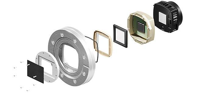
To fulfill these requirements, XIMEA chose for its design to incorporate Peltier-cooled scientific CMOS (sCMOS) sensors protected behind a standard DN 63 CF vacuum flange (Figure 1). The approach allows for additional flange formats.
The selected detector component comes from Gpixel’s PulSar line of backside-illuminated scientific CMOS sensors, which are designed to detect photons from the ultraviolet through soft x-ray range with high quantum efficiency. The sensor technology builds on earlier iterations by implementing minor changes to the sensor’s backside fabrication process. Specifically, the process eliminates the antireflection coating, leaving no remaining dielectric films. It also reduces the sensor’s dead layer from 27 to 5 nm and increases the thickness of the silicon layer from 3.5 to 9.5 µm to suppress radiation damage. The incorporation of boron in the sensor material serves to decrease the implantation of energy. This reduces dark counts and readout noise from the sensor backside and leads to enhanced sensitivity for wavelengths toward the lower end of the spectrum.
The sensitivity of the Gpixel sensor is slightly reduced in the UV-visible range compared to the sensor’s base model. This is most likely attributable to the backside fabrication process applied. Yet, the sensor specified for XIMEA’s camera still shows extraordinary sensitivity, with quantum efficiency exceeding 90% in the high energy ranges.
The camera design specified a fast USB 3.1 Gen1 interface with USB-C connection and power delivery from a PD 2.0-enabled host. XIMEA’s design approach also emphasized a compact footprint measuring roughly 52 × 52 × 61.75 mm (HWD) and weighing 336 g, excluding the vacuum flange. Together with its highly durable seals and active Peltier cooling to keep the sensor temperature below −20 °C, the camera design meets nearly all instrumental requirements, enabling improved detection in a versatile range of scientific and industrial applications.
High-energy applications
A wide range of scientific techniques and industrial applications are fueling interest in imaging technologies able to enhance EUV and soft x-ray detection. For example, as the semiconductor industry continues to achieve evermore advanced nodes, it will require further advancements in EUV ptychography and EUV spectroscopy to overcome the diffraction limit and resolve even smaller structural features.
Microscopic imaging and tomographic techniques for life science applications will also benefit from cameras delivering high sensitivity — particularly in the soft x-ray domain. Specifically, techniques such as scanning transmission x-ray microscopy and x-ray photoemission electron microscopy could become even more suited to visualize and quantify mesoscale biology in planar- and 3D-image reconstruction.
Moreover, many chemical gases and biologically relevant molecules have spectral signatures in the soft x-ray and UV regimes. Camera advancements targeting these spectral ranges could consequently improve analytical techniques such as soft x-ray absorption spectroscopy, near-edge structure spectroscopy, and UV-Raman spectroscopy. These improvements would translate to many end applications for these techniques in forensics, plant science, astronomy, solar imaging, atmospheric chemistry, and the entire life sciences sector.
Beyond these potential end uses, there is another ongoing trend toward the integration of well-established imaging techniques with spectroscopic instrumentation to achieve correlative microscopy. Enabling this technology with EUV and soft x-ray sensitivity would increase the efficiency of single measurements by covering a wider wavelength band per shot. As new camera designs targeting the EUV and soft x-ray wavelength ranges expand end-use possibilities, advancements in the component technologies themselves will lend further momentum to the technology’s adoption. Such cameras would benefit from expanding sensor diversity, as well as new modifications to mechanics such as interface, cabling, and camera form factors. Like the photons typifying the EUV and soft x-ray bands, the technologies and applications populating these regimes are exhibiting high energy.
Meet the authors
Jan-Hendrik Budde is a key account manager at XIMEA GmbH. In addition to earning a diploma in biophysics from Rhineland-Palatinate Technical University of Kaiserslautern-Landau, his expertise includes advanced photonics technologies; email: jan.budde@ximea.com.
Michael Cmok is managing director at XIMEA GmbH. His background includes expertise in image processing, computer graphics, and artificial intelligence. Cmok earned his diploma in computer science from the University of Koblenz and Landau; email: michael.cmok@ximea.com.
Trendsetting high-performance cameras since 1992. Based in Münster (GER), XIMEA serves all types of tech companies around the world, from global players to small start-ups. Known as a reliable and professional innovator, developer, and distributor in the markets of industrial and scientific imaging. The product portfolio ranges from high-performance cameras, multi-camera systems to miniature cameras for demanding challenges in the field of machine vision. Especially compact formfactors, low latencies, and power consumption as well as super-fast interfaces and high resolutions are the core competencies. XIMEA´s camera technologies allow the customers to improve their products and to enable their applications. Facing challenges together with clients to solve individual needs with standard products and custom designs, is an essential philosophy of XIMEA. With more than 25 years of experience the engineers of XIMEA are constantly setting new standards for the entire industry through designing solutions for OEM-projects and OTS-products. Virtual reality, industrial, scientific, embedded applications and many other sectors benefit from these innovative cameras and software tools. The personal service approach is supposed to support system integrators and engineers to achieve highest effectivity.
XIMEA GmbH
Am Mittelhafen 16
48155 Münster
Telefon: +49 (251) 202408-0
Telefax: +49 (251) 202408-99
http://www.ximea.com
![]()