Hamamatsu Photonics has developed a high-sensitivity, high-resolution semiconductor failure analysis system that utilizes visible to near-infrared light, all in just a single unit
Brief look at PHEMOS-X
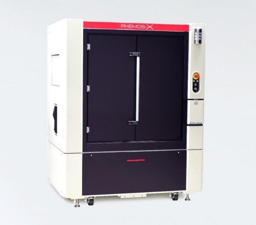
The PHEMOS-X is a semiconductor failure analysis system that can be equipped with up to five lasers having different output wavelengths from visible to near-infrared light. With just a single unit, the PHEMOS can localize failures with high sensitivity and high resolution.
When a voltage is applied to a semiconductor device, the failure points in the semiconductor device emit light and heat. Scanning a semiconductor device with a laser beam while a voltage is applied to it causes the electrical current and operating state at the failure location to change. By utilizing these properties, the failure location can be estimated by detecting signals that represent changes in the semiconductor device caused by the applied voltage, laser scanning and visualizing those signals as images. At Hamamatsu Photonics we develop, manufacture and sell semiconductor failure analysis systems for various semiconductor devices in order to meet customer demands that vary with the constant advances made in semiconductor devices.
By applying our in-house optical design technology, we have redesigned the components of the analysis system from scratch such as the laser scanner for scanning a semiconductor device with a laser beam, the optical stage for positioning a semiconductor device, and the macro lens for wide field-of-view observation. This has led to higher sensitivity, resolution, accuracy and better ease-of-use which are significantly improved features compared to our current system.
Conventional laser scanners are specifically designed for near-infrared light at a wavelength of 1300 nanometers (a nanometer, or nm, is one billionth of a meter). This time we redesigned the optical system and succeeded in developing a laser scanner that suppresses optical loss in the 5 lasers it can contain. As a result, semiconductor failure analysis can be performed with just one unit, utilizing multi-wavelength laser beams from visible light of 532 nm to near-infrared light of 1340 nm. Using a laser with a shorter wavelength before what allows observation of semiconductor devices in more detail. It also ensures high sensitivity for finding and observing the failure points in power semiconductors that respond to visible light, rather than infrared light to which ordinary semiconductors respond.
At the same time, we increased the laser irradiation intensity so that the signal quantity representing changes in the electrical current and operating state at the failure point becomes larger, allowing even higher sensitivity observation. We also reviewed the optical design of the macro lens to increase the aperture ratio which enables the detection of even lower light emissions. Moreover, we improved the positioning accuracy and repeatability of the optical stage by employing a drive mechanism capable of precise manipulation as well as redesigning the laser scanner to enhance the positioning accuracy of the irradiation point, so that the failure points can be observed more accurately. The systems usability has also been improved by redesigning the equipment structure and developing software to use a touch panel for easy, intuitive operation.
In just a single unit, the PHEMOS-X can handle multi-wavelength laser light to perform analysis with high sensitivity, high resolution and high accuracy. Yet the PHEMOS-X is still easy to use and helps localize failures in a broad range of semiconductor devices such as state-of-the-art semiconductor devices and power semiconductors that are likely to rapidly grow in demand. This also makes the PHEMOS-X a promising tool that will enhance the efficiency of analysis tasks.
We will continue to develop failure analysis systems and their options to meet customer needs.
Failure analysis flow
First, a semiconductor tester electrically estimates the area where a failure is occurring. The PHEMOS-X then narrows down the failure area to a precise site. Finally, the device is cut along the estimated failure site and the cross section observed with an electron microscope to identify the failure position.
Features of PHEMOS-X
1. Improved sensitivity from newly developed multi-wavelength laser scanner and highly efficient macro lens
Conventional laser scanners are designed specifically for near-infrared light at wavelength of 1300 nm. This time we redesigned the optical system to optimize the lens layout and mirror coating and succeeded in developing a laser scanner that suppresses the optical loss of 5 lasers mountable in the unit. This increased the intensity of multi-wavelength laser beams from visible light at 532 nm to near-infrared light at 1340 nm, so that the signal quantity representing changes in the electrical current and operating state at the failure point becomes large enough to enable observation with even higher sensitivity. In most cases, a wide field-of-view macro lens is used to analyze the defects in semiconductor devices in relatively large sizes such as semiconductor memories. However, this time we redesigned the macro lens to increase its aperture ratio by 120% compared to a conventional lens, thereby allowing detection of even lower light emissions. At the same time, we also improved the optical design for highly sensitive detection of changes in the electrical current and operating state at the failure point, which are induced by laser scanning.
2. Improved spatial resolution thanks to a multi-wavelength laser scanner
The shorter the laser light wavelength, the smaller the irradiated area. The optical system of conventional laser scanners is specifically designed for near-infrared light. However, our newly developed laser scanner is compatible with visible light up to the 532 nm wavelength, which allows the use of a visible laser to localize failures in more detail.
3. Improved positioning accuracy and repeatability
Positioning accuracy is the difference between the target point of the optical stage and actual stop position. We have employed a drive mechanism capable of high-precision manipulation that improves positioning accuracy up to 10 times that of conventional products. At the same time, the stop position repeatability has been increased approximately 4 times. We also revamped the laser scanner design to enhance the positioning accuracy of the laser irradiation point so that failures can be localized more accurately.
4. Better ease-of-use due to the redesigned structure and software development
We redesigned the equipment structure and optical stage including the peripheral components to make it easier to do tasks such as semiconductor device positioning. We also developed software that can display and join multiple images together which will improve the equipment usability and work efficiency.
Background of PHEMOS-X development
Countless semiconductor devices are incorporated into a diverse range of products including personal computers, smartphones, industrial equipment and cars. These must exhibit high reliability or, in other words, must operate and function correctly for a certain period of time under given conditions. Because of this requirement, semiconductor device manufacturers are testing their devices to find internal defects and clarify their cause starting from the defect position. Then, based on the analysis results, they improve the device design and production processes to increase reliability. In the future, with the spread of 5th generation mobile communication systems (5G) and cloud services, semiconductor devices are likely to need further “die shrinks” in order to improve the processing capacity per area. In the field of next-generation vehicles such as electric vehicles (EV), the focus is on high-efficiency power semiconductors made of compounds such as silicon carbide (SiC) and gallium nitride (GaN). This is increasing the demand for failure analysis systems that can localize failures faster and more efficiently.
Hamamatsu Photonics Deutschland GmbH
Arzberger Str. 10
82211 Herrsching am Ammersee
Telefon: +49 (8152) 375-0
Telefax: +49 (8152) 375-199
http://www.hamamatsu.com
![]()